The specifications on distortion have become more severe in most signal processing circuits such as communication systems, sensor systems, etc. Distortion can be reduced by proper choice of operation points of the transistors in the frontends, and by feedback. Distortion can also be cancelled if sufficient levels of matching can be achieved.
In this tutorial the several specifications of distortion are reviewed. This is followed by an optimization of the input transistor operating points for low distortion. The effect of feedback on distortion is discussed next. Finally distortion cancellation scheme’s are discussed as used in LNA’s and other frontend circuits.
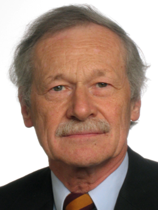
Willy Sansen has received a PhD degree from the UC Berkeley in 1972. He went back to the KULeuven, where he became full professor in 1980. During 1984-2008 he has headed the ESAT-MICAS laboratory on analog design. Prof. Sansen is a member of several editorial and program committees of journals and conferences. He was Program chair of the ISSC conference in 2002 and President of the Solid-State Circuits Society in 2008-2009. He is recipient of the SSCS Donald Pederson Award in 2011. He is a Life Fellow of the IEEE
He has been supervisor of over sixty-five PhD theses in the discipline of analog design. He has authored and coauthored more than 650 and sixteen books among which the slide based book “Analog Design Essentials” (Springer 2006).

There are several medical devices are made to monitor their heart to avert the heart diseases. Moreover, body sensor networks (BSNs) based applications or wearable devices have become more acceptable to the people for monitoring the real-time health information, such as the electrocardiogram (ECG). In order to enhance the portability of BSNs, a low-power wireless ECG acquisition system on a chip (SOC) stuck on the body is required. In this tutorial, a bio-signal acquisition system with the features of low power consumption, wireless transmission, and the on-time monitoring will be presented. Moreover, some researches have been reported that it is efficient to electrically generate neural action potential to control dysfunctional organs. Therefore, the telemetry integrated circuits will be required because they can provide coupling power and are able to transmit or receive data to or from according to implantable body sensor network. In this tutorial, a closed-loop implantable micro-stimulator system on chip (IMSoC), which possesses the sensing of a physiological signal, micro-stimulation, and wireless data/command transmission, will be also presented.
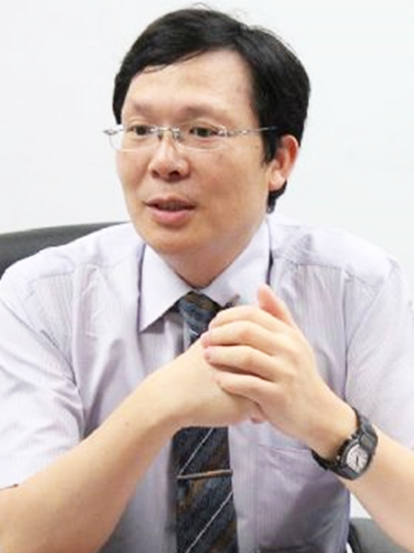
Shuenn-Yuh Lee received the B.S. degree from the National Taiwan Ocean University, Keelung, Taiwan, in 1988, and the M.S. and Ph.D. degrees from the National Cheng Kung University, Tainan, Taiwan, in 1994 and 1999, respectively. He is currently a Professor at the Department of Electrical Engineering, National Cheng Kung University, Tainan, Taiwan. From 2013 to 2016, he serves as the Chairman of IEEE Solid-State Circuits Society Tainan Chapter. From 2016 to 2017, he serves as the Vice Chairman of IEEE Tainan Section. He is the Associate Editor of IEEE Transaction on Biomedical Circuits and Systems from 2016-2019. His present research activities involve the design of analog and mixed-signal integrated circuits, biomedical circuits and systems, low-power and low-voltage analog circuits, and RF front-end integrated circuits for wireless communications.

The fifth generation (5G) is about to begin in 2020. New applications are expected in 5G where data rate of 10 Gb/s and low delay of 1 ms are realized. Meanwhile, discussion on "Beyond 5G" after 10 years is beginning to start, since the mobile generation has evolved every decade.
The need for high-speed communication continues in the future since the data handled over the Internet is exponentially increasing. How can we realize the target communication speed of 100 Gb/s in Beyond 5G? One powerful candidate is a new communication technology using the 300-GHz band which is one of the terahertz bands. In this presentation, firstly, the evolution of communication speed is introduced, and the reason why wireless communication has dramatically increased the data rate will be discussed. Then, after the superiority of the 300-GHz band usable for wireless communication is introduced, CMOS technology for realizing the 300-GHz-band wireless communication is explained. Finally, how the world changes with beyond 5G using terahertz communication will be discussed.
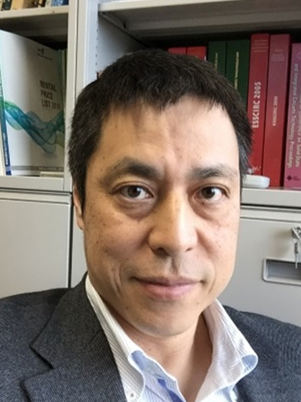
Minoru Fujishima received the B.E., M.E. and Ph.D degrees in Electronics Engineering from the University of Tokyo, Japan in 1988, 1990 and 1993, respectively. He joined faculty of the University of Tokyo in 1988 as a research associate, and was an associate professor of the School of Frontier Sciences, University of Tokyo since 1999. He was a visiting professor at the ESAT-MICAS laboratory, Katholieke, Universiteit Leuven, Belgium, from 1998 to 2000. Since 2009, he has been a professor of the Graduate School of Advanced Sciences of Matter, Hiroshima University.
He studied design and modeling of CMOS and BiCMOS circuits, nonlinear circuits, single-electron circuits, and quantum-computing circuits. His current research interests are in the designs of low-power millimeter- and short-millimeter-wave wireless CMOS circuits. He coauthored more than 50 journal papers and 120 conference papers. He served as a distinguished lecturer in IEEE solid-state circuits society from 2011 to 2012.

Now, it is the era of deep learning and AI. Among various approaches to accelerate neural network calculation, HBM (high bandwidth memory) DRAM is one of key components in a state-of-the-art accelerators.
Basically, HBM DRAM shows unparalleled bandwidth like 1TB/s in a small SiP (system in package). To provide this huge bandwidth, there are many challenges like power density, thermal dissipation, testability and reliability from stacking and 2.5D configuration.
In this tutorial, the reasons for using HBM in accelerators are explained in detail, and the key schemes of HBM and difficulties of developing and using HBM will be discussed. Furthermore, the requirement of memory system for next generation AI and the promising features including near data processing are also touched.
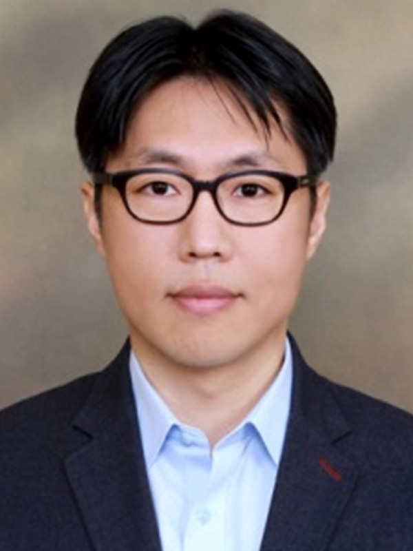
Kyomin Sohn received the B.S. and M.S. degrees in Electrical Engineering in 1994 and 1996, respectively, from Yonsei University, Seoul. From 1996 to 2003, he was with Samsung Electronics, Korea, involved in SRAM Design Team. He designed various kinds of high-speed SRAM devices.
He received the Ph.D. degree in EECS in 2007 from KAIST, Daejeon, Korea. He rejoined Samsung Electronics in 2007, where he has been involved in DRAM Design Team. He is a Master (Technical VP) in Samsung and he is responsible for development of HBM DRAM and Future Technology.
His interests include the next generation 3D-DRAM, robust memory design, and processing-in-memory for AI applications. Since 2012, he has currently served as a Technical Program Committee member of Symposium on VLSI Circuits.